 Invited Review on “Computational modeling of nanoparticle coalescence“
- P. Grammatikopoulos, M. Sowwan, and J. Kioseoglou
Computational Modeling of Nanoparticle Coalescence
Advanced Theory and Simulations, 2(6) 1900013, (2019)
link

Workshop “Computational Materials Science”

Invited Review on “Computational modeling of nanoparticle coalescence“
featured in the inside front cover of the issue.
- P. Grammatikopoulos, M. Sowwan, and J. Kioseoglou
Computational Modeling of Nanoparticle Coalescence
Advanced Theory and Simulations, 2(6) 1900013, (2019)
link
featured on the inside back cover of the issue
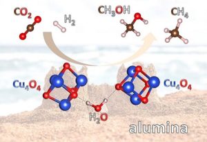
- A. Halder, J. Kioseoglou, B. Yang, K. L. Kolipaka, S. Seifert, M. Pellin, M. Sowwan, S. Vajda, P. Grammatikopoulos
Nanoassemblies of ultrasmall clusters with remarkable activity in carbon dioxide conversion into C1 fuels
Nanoscale 11, 4683-4687 (2019),
link
Graphical abstract
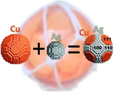
- Panagiotis Grammatikopoulos, Joseph Kioseoglou, Antony Galea, Jerome Vernieres, Maria Benelmekki, Rosa E. Diaz and Mukhles Sowwan
Kinetic trapping through coalescence and the formation of patterned Ag–Cu nanoparticles
Nanoscale, 2016, 8, 9780-9790
link


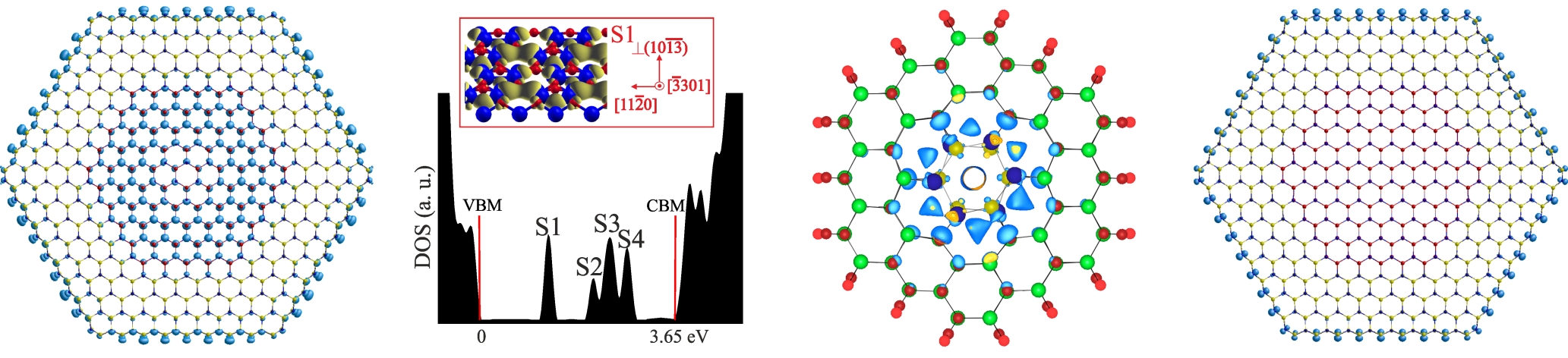
(a) Displacement magnitude compared to the relaxed GaN NW, (b) the average stress along the and directions for the various shell-to-NW ratios examined and (c) the excess energy per atom for the various shell-to-NW examined. In all the cases the atoms are colored according to the individual parameter that is calculated by the IP and following the corresponding color bar.
- Pavloudis, T., Termentzidis, K., Komninou, P., Latham, C.D., Briddon, P.R., Kioseoglou, J.
The influence of structural characteristics on the electronic and thermal properties of GaN/AlN core/shell nanowires
Journal of Applied Physics, 2016, 119, 7, 074304
link

Charge density distribution isosurfaces at the Γ-point of the main states: (a) the VBM, (b) the CBM, and (c) the lowest unoccupied states above the CBM. Red spheres denote Ga, yellow are Al, and blue are N atoms.
- Pavloudis, T., Termentzidis, K., Komninou, P., Latham, C.D., Briddon, P.R., Kioseoglou, J.
The influence of structural characteristics on the electronic and thermal properties of GaN/AlN core/shell nanowires
Journal of Applied Physics, 2016, 119, 7, 074304
link

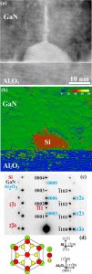
(a) Cross-sectional HRTEM image of the GaN/Al2O3 interface, along the [11-20]GaN zone axis. (b) Map of out-of-plane GPA strain component calculated from (a).(c)Common SAED pattern of the three structures, along the [11-20]GaN//[1-100]Al2O3//[112]Si zone axes(d) Atomistic structural model of the observed epitaxial relationship between Si and Al2O3, projected along [-1-11]Si//[0001] Al2O3.
- Koukoula, T. and Kioseoglou, J. and Kehagias, T. and Furtmayr, F. and Eickhoff, M. and Kirmse, H. and Karakostas, T. and Komninou, P.
Interfacial properties of self-assembled GaN nanowires on pre-processed Al2O3(0001) surfaces
Materials Science in Semiconductor Processing, 2016, ,
link

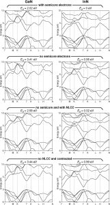
The calculated band structures of wurtzite GaN (left) and InN (right). The topmost pair of graphs shows the results with uncontracted basis HGH pseudopotentials that include the Ga-3d and In-4d semicore electrons explicitly; the second pair shows the results with uncontracted basis and HGH pseudopotentials; the third pair shows results with uncontracted basis and HGH pseudopotentials with a non-linear-corecorrection, and the fourth pair shows results with contracted basis HGH pseudopotentials.
- Kioseoglou, J., Pavloudis, T., Kehagias, T., Komninou, P., Karakostas, T., Latham, C.D., Rayson, M.J., Briddon, P.R., Eickhoff, M.
Structural and electronic properties of GaN nanowires with embedded InxGa1-xN nanodisks
Journal of Applied Physics, 2015, 118, 3, 034301
link

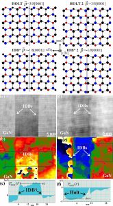
Atomistic models of the {10-10} IDBs in wurtzite III-N, projected along the [11-20] direction. The boundary plane is indicated by a solid line, large and small (red) circles denote III and N atoms, respectively, light-shaded (blue) circles are at 0 level and dark (black) circles are at level a/2 along the projection direction. By convention, “III-polarity” corresponds to growth along [0001]//III-N bond. (a)-(d) HRTEM images of IDs in the GaN layer along the [11-20] zone axis. (b)-(e) Corresponding phase images using the 0002 g vector and the 0001 g vector in FFT, respectively. (c)-(f) Line profiles of the phase images perpendicular to the IDBs. The integration width of each profile is marked on the phase images. Based on the value of the phase shift between the adjacent inverse polarity domains, IDB* and Holt IDBs are identified in (c) and (f), respectively.
- Koukoula, T., Kioseoglou, J., Kehagias, T., Ajagunna, A.O., Komninou, P., Georgakilas, A.
Self-annihilation of inversion domains by high energy defects in III-Nitrides
Applied Physics Letters, 2014, 104, 14, 141914
link